Technology Overview
Nanoscience Enabled
Scientists have wrestled for decades to establish cost effective processes to convert sunlight into energy. In 2002, Nanosolar set out to revolutionize the solar energy manufacturing processes and by 2010 Nanosolar had the first solar modules ready for field installations. Our proprietary approach to printing CIGS (Copper, Indium, Gallium, Selenium) and nanoparticle inks minimizes our use of expensive, high vacuum manufacturing equipment.
Nanosolar has achieved 17.1% efficiency on laboratory devices, certified by NREL, which shows the potential of our technology to compete with the efficiency of crystalline silicon panels in the next several years. Moreover, the Nanosolar Utility Panel’s innovative design significantly reduces balance-of-system costs through less mounting hardware, electrical cabling and installation labor.
Technological innovation on solar cell level
- Use of a highly conductive, low-cost aluminum foil as the substrate and bottom electrode of the cell
- CIGS ink with pre-defined ratio and a high-yield, high-throughput printing process to form an electronic-grade CIGS semiconductor
- Novel Metal-Wrap-Through (MWT) back-contact design based on high-throughput foil lamination
- Thin/printed transparent top electrode
High-throughput roll-to-roll printable semiconductor technology to enable the world’s lowest-cost thin-film solar panels
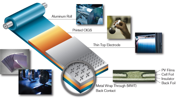 The result of the front-end cell production is a roll of inexpensive aluminum foil substrate coated with multiple thin film layers totalling less than two microns. Our printed CIGS solar cells and panels are on track to reach efficiencies competitive with crystalline silicon panels in the next several years. Moreover, the Nanosolar Utility Panel’s innovative design significantly reduces balance-of-system costs through less mounting hardware, electrical cabling and installation labor. The end result is a lower levelized cost of energy than competing solar technologies.